Leader: Swapan Gayen
Members: Daniel Akins, Ubaldo Cordova-Figueroa, Pouyan Ghaemi, John Lombardi, Gustavo Lopez, Vinod Menon, Carlos Meriles, Kyungwha Park, Mark Shattuck, Maria Tamargo, Jacob Trevino
Collaborators: Anthony Johnson (University of Maryland Baltimore County) Thomas Myers (Texas State University), M. Leona (Metropolitan Museum of Art), Y. S. Hor (Missouri S&T), G. Kahl (TU Vienna) and C. Likos (Vienna University), J. Wrachtrup (Universitat Stuttgart)=
Subproject 3 has two major thrusts in nanomaterials study. First, developing and adapting versatile experimental approaches and sensors for nanomaterials characterization. Second, using and implementing proper analytical and numerical methods for developing detailed understanding of the mechanisms and parameters that affect nanomaterial properties. The ultimate goal is to be able to formulate selection and design criteria for these materials a priori. The activities of Subproject 3 are organized in following three clusters.
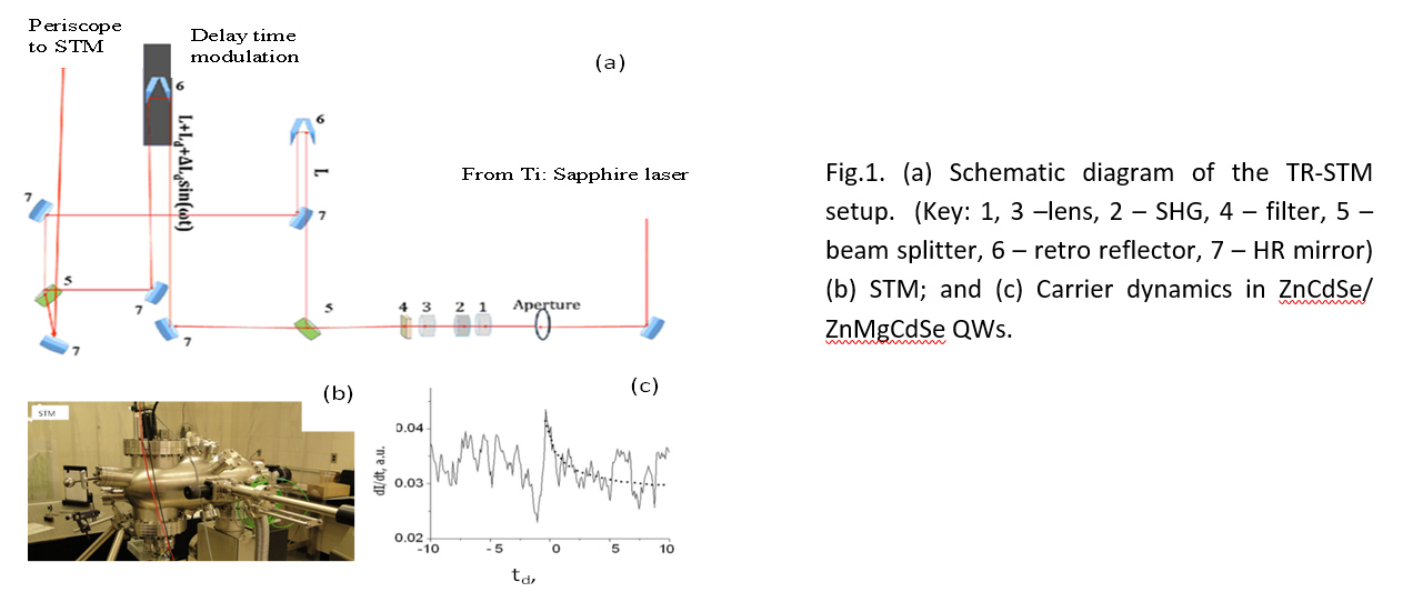
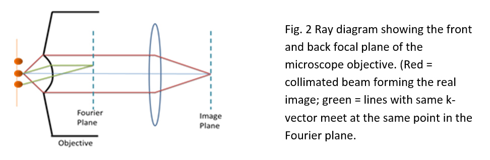
Cluster 3.1:Sensitive probes and characterization methods: In addition to using standard steady-state, time-resolved, and nonlinear optical methods for study of nanomaterials being developed in Subprojects 1 and 2, a major thrust here is to develop and adapt emerging techniques, such as, ultrafast time-resolved scanning tunneling microscopy (STM) and spectroscopy[1] and Fourier space imaging and near-field microscopy [2] for study of layered surfaces and interfaces; and to explore Surface-Enhanced Raman Scattering (SERS) [3] for innovative sensing and probing applications.
Cluster 3.2. Analytical approaches and numerical modelling for materials study and design: Our team uses analytical and numerical methods for study of materials and to provide guidance for new materials synthesis and functionality enhancement to the other subprojects. Quantum Field Theory (QFT) based approaches are adapted to help develop and study topological insulators, as well as, investigate quantum transport in different 2-Delectron systems [4]. First-principles calculations using density-functional theory (DFT) are being carried out to elucidate properties of semiconductor quantum structures of Subproject 1 [5-8]. Other numerical approaches (such as, Quantum Mechanics/Molecular Mechanics numerical methods[9], Monte Carlo algorithms, finite difference methods, boundary element method, and Brownian dynamics) are adapted and used to help design and characterize novel peptides, patchy particles and reconfigurable structures studied in Subproject 2.
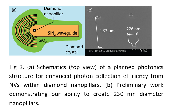
Cluster 3.3. “Spin complexes” for sensing and quantum information processing: The so-called ‘spin complexes’ comprise a paramagnetic center, typically in the form of an atomic defect in a crystal, and neighboring nuclear spins, such as, nitrogen vacancy (NV) center in diamond [10]. Spin control at the nanoscale is emerging as a key technology area [11] with applications ranging from high-resolution sensing to quantum information processing. Using the NV center in diamond as the central material platform, this cluster utilizes nanofabrication and single spin control to: (a) explore photonic and phononic metastructures for enhanced single spin manipulation; (b) investigate dynamic nuclear spin polarization in liquids via cross-relaxation with NV centers; and (c) locally probe various material properties (magnetic, electrical, thermal) with nanoscale resolution.
References:
- M. Yamashita, H. Shigekawa, R. Morita (Eds.), Monocycle Photonics and Optical Spanning Tunneling Microscopy, Springer, 2005.
- M. A. Lieb, J. M. Zavislan, and L. Novotny, Single-molecule orientations determined by direct emission pattern imaging, J. Opt. Soc. Am. B 21, 1210 (2004).
- J.R. Lombardi, R.L. Birke, The Theory of Surface-Enhanced Raman Scattering in Semiconductors, J. Phys. Chem. C 118, 11120 (2014), doi.org/10.1021/jp5020675.
- Y. I. Joe, X. M. Chen, P. Ghaemi, K. D. Finkelstein, G. A. de la Peña, Y. Gan, J. C. T. Lee, S. Yuan, J. Geck, G. J. MacDougall, T. C. Chiang, S. L. Cooper, E. Fradkin, P. Abbamonte, Emergence of charge density wave domain walls above the superconducting above the superconducting dome in 1T-TiSe2, Nat. Phys. 10, 421 (2014).
- G. Kresse and D. Joubert, From ultrasoft pseudopotentials to the projector augmented-wave method, Phys. Rev. B 59, 1758 (1999).
- J. P. Perdew, K. Burke, and M. Ernzerhof, Generalized Gradient Approximation Made Simple, Phys. Rev. Lett. 77, 3865 (1996).
- Y. Hinuma, A. Gruneis, G. Kresse, and F. Oba, Band alignment of semiconductors from density-functional theory and many-body perturbation theory, Phys. Rev. B 90, 155405 (2014).
- G.E. Lopez, I. Colon, A. Cruz, S. Ghosh, S.B. Nicholis, U. Viswanethan, S.M. Auerbach, and S.M. Hardy, Modeling non-aqueous proton wires tethered to helical-peptides: Biased proton transfer driven by helical dipoles, J. Phys. Chem. A 116, 1283 (2012).
- V. Acosta, P. Hemmer, “Nitrogen-vacancy centers: Physics and applications,” MRS Bulletin 38, 127 (2013).
- A. Laraoui, F. Dolde, C. Burk, F. Reinhard, J. Wrachtrup, C. A. Meriles, “High-Resolution Correlation Spectroscopy of 13C Spins Near a Nitrogen-Vacancy Center in Diamond”, Nat. Commun. 4, 1651 (2013).
- Z. Chen, L. Zhao, K. Park, T. A. Garcia, M. C. Tamargo, and L. Krusin-Elbaum, Robust Topological Interfaces and Charge Transfer in Epitaxial Bi2Se3/II−VI Semiconductor Superlattices, Nano Letters 15, 6365-6370 (2015)