Leader: Swapan Gayen
Team: Gayen, Begliarbekov, Braunschweig, Dorsinville, Eisele, Khanikaev, Lombardi, Menon, Shen, Tamargo.
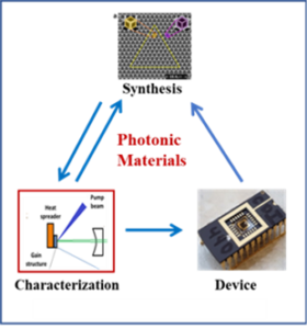
Subproject 3 is designed to explore emerging basic ideas, synthesize new materials with unprecedented functionalities, investigate salient properties of the engineered materials, design and test devices based on promising materials, and provide feedback for materials and device design criteria. New in IDEALS II, it will organize this synergistic interplay between bold basic concepts and technological advances in three clusters: (i) Topological photonics and entangled photons; (ii) Photonic phenomena in hybrid materials; and (iii) Semiconductor nanostructures for next-generation photonic devices. The proposed activities align with national priorities of quantum optics, energy sources and sensors.
Cluster 1. Topological photonics and entangled photons will explore emerging quantum phenomena in photonic systems, such as topological metasurfaces1 and exciton-polaritons2 to achieve non-trivial control of strong light-matter interaction. Photonic systems based on 2D transition metal dichalcogenides (TMDs) and epitaxial semiconductor quantum structures, as well as topological photonic nanostructures integrating organic molecules will be fabricated, and quantum optic phenomena arising in these structures from strong light-matter interactions will be investigated and their potential applications explored. This Cluster will also develop a polarization sensitive quantum optical coherence tomography (QOCT) approach using entangled photons and surface plasmon polaritons (SPPs) for imaging and characterizing materials surfaces including metamaterials and biological cells and tissues, with useful application in the cancer diagnostic effort in Subproject 2.
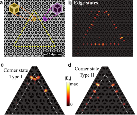
Near-field imaging of first- and higher-order topological boundary states: (a) Metasurface showing the topological domain surrounded by the trivial domain. (b) Near-field distribution of the topological edge states at 6.24 µm, (c) Near-field of Type-I corner state, and, (d) Near-field of Type-II topological corner state induced by the long-range interactions at 6.205 µm.
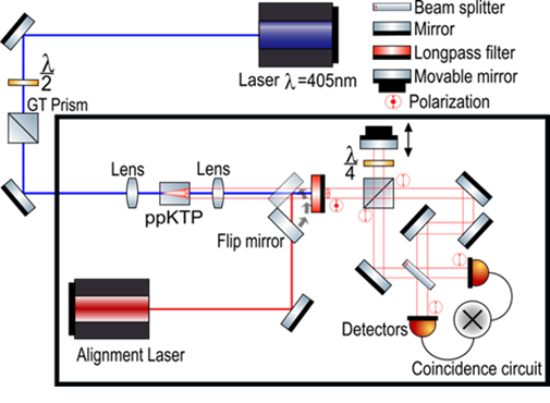
Schematic of the proposed Quantum optical coherence tomography (QOCT) system.
Cluster 2. Photonic phenomena in hybrid materials: II-VI/III-V semiconductor heterovalent structures and 3D/2D hybrid materials combine materials not typically found in a single structure, thus expanding the materials properties and capabilities in unprecedented directions.3,4 Various monolithic hybrid structures comprising these heterointerfaces will be grown and their properties investigated by advanced structural and spectroscopic probes. Device potential will be explored and realized. Surface enhanced Raman spectroscopy (SERS) of molecules adsorbed on semiconductor surfaces was explored in IDEALS I for homeland security and other applications,5 and a method for assessing the degree of charge transfer was introduced6 enhancing SERS’ dexterity. In IDEALS II, we will extend this research to other semiconductor surfaces, starting with variously etched GaN, GaAs, TiO2, ZnO; but also including organic surfaces such as supra-molecular organic semiconductor thin films and self-assembled nanotube J-aggregates being pursued in Subproject 2.
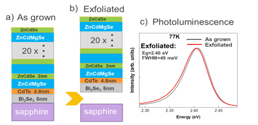
Hybrid materials: a) ZnCdSe/ZnCdMgSe MQW structure grown on a CdTe/Bi2Se3/sapphire virtual substrate by MBE. b) MQW structure exfoliated using the “scotch tape” technique. c) Comparison of the 77K PL of the as-grown and exfoliated samples.
Cluster 3. Semiconductor nanostructures for next-generation photonic devices: IDEALS I research made important strides in the development of II-VI semiconductor heterostructures (SHSs) with potential applications in quantum cascade detectors and emitters7 and intermediate band solar cells (IBSC).8 IDEALS II research will further exploit the team’s leading expertise in II-VI and III-V SHSs using molecular beam epitaxy (MBE) and focus on the demonstration of working devices from these materials. We will design, grow and fabricate high efficiency IBSC based on type II quantum dots, and high brightness optically-pumped SDLs based on ZnxCdyMg1-x-ySe/ZnCdSe multiple quantum well structures with fundamental emission in the so-called green and yellow spectral range “gap”.9.10 Another thrust will explore the plasma-assisted MBE growth of novel oxide semiconductors, such as, ZnO11 Ga2O312 and MnO13 (Shen) for quantum device and opto-electronic applications. Advanced characterization of the structural and spectroscopic properties of the materials will include x-ray diffraction, transmission electron microscopy, photoluminescence (PL) and excite-and-probe techniques.
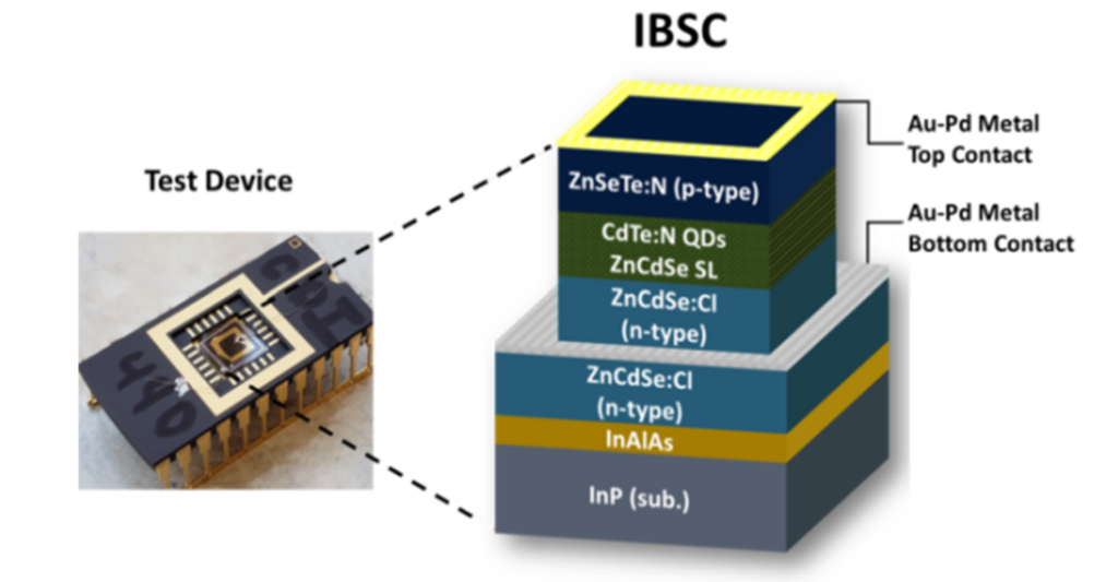
Proposed Type-II QD IBSC device structure. Left: Test device mounted on a chip for testing.
References:
- Li , D. Zhirihin, M. Gorlach , X. Ni, D. Filonov, A. Slobozhanyuk, A. Alu, A. B. Khanikaev, “Higher-order topological states in photonic Kagome crystals with long-range interactions”, Nat. Photonics 14, 89-94 (2020).
- Liu, T. Galfsky, Z. Sun, F. Xia, E. Lin, Y.H. Lee, S. Kéna-Cohen, V.M. Menon, Strong light–matter coupling in two-dimensional atomic crystals, Nat. Photonics 9, 30-34 (2015).
- Chen, L. Zhao, K. Park, T. A. Garcia, M. C. Tamargo, and L. Krusin-Elbaum, Robust Topological Interfaces and Charge Transfer in Epitaxial Bi2Se3/II−VI Semiconductor Superlattices, Nano Letters 15, 6365 (2015)
- Kaya, S. Kacmoli, M. S. Claro, T. A. Garcia, C. Forrester, V. Deligiannakis, M. C. Tamargo, and C. Gmachl, Hybrid II-VI/III-V Intersubband Detectors, IQCLSW 2018, 2-7 Sep 2018 Cassis (France)
- Haddad, M. A. Comanescu, O. Green, T. A. Kubic, and J. R. Lombardi, Detection and Quantitation of Trace Fentanyl in Heroin by Surface Enhanced Raman Spectroscopy, Anal. Chem. 90, 12678 (2018).
- Omari Kirkland, Jan L. Weyher, John R. Lombardi, Charge-Transfer Mapping of Nanostructured GaN/Ag Surfaces using Surface Enhanced Raman Spectroscopy, Spectrosc. 110, 103106 (2020).
- A. Garcia, J. De Jesus, A. P. Ravikumar, C. F. Gmachl, and M. C. Tamargo, II–VI quantum cascade emitters in the 6–8 µm range, Phys. Status Solidi b 253, 1494 (2016)
- Deligiannakis, G. Ranepura, I. L. Kuskovsky, and M. C. Tamargo, Advanced material system for the design of an intermediate band solar cell: Type-II CdTe quantum dots in a ZnCdSe matrix, J. Appl. Phys. 126, 235302 (2019)
- De Jesus, T. A. Garcia, V. Kartazaev, B. E. Jones, P. J. Schlosser, S. K. Gayen, J. E. Hastie, and M. C. Tamargo, Growth and characterization of ZnCdMgSe-based green light emitters and distributed Bragg reflectors towards II–VI based semiconductor disk lasers, Phys. Status Solidi A 212, 382 (2015).
- Zhao, V. Kartazaev, G. Chappell, J. Hastie, S. K. Gayen, and M. Tamargo, Gain measurements of Se-based II-VI multiple quantum well structures for vertical-external-cavity surface-emitting laser applications, presented at the 35th North American MBE Conference, Ketchum, ID, 2019
- Zhao, G. Chen, B.-S. Li, and A. Shen, Mid-infrared intersubband absorptions in ZnO/ZnMgO multiple quantum wells, Applied Physics Letters 104, 212104 (2014)
- Zhang, J. Shi, D.-C. Qi, L. Chen, and K. H. L. Zhang, Recent progress on the electronic structure, defect, and doping properties of Ga2O3, APL Mater.8, 020906 (2020)
- K. Kundu, K.S.R. Menon, Growth and characterization of ultrathin epitaxial MnO film on Ag (001), J. Crystal Growth 446, 85, (2016)