Leader: Lia Krusin-Elbaum
Members: Swapan Gayen, Pouyan Ghaemi, Lia Krusin-Elbaum, Gustavo Lopez, Vinod Menon, Kyungwha Park, Aidong Shen, Maria Tamargo and Jacob Trevino
External collaborators: James Hone (Columbia University), Claire Gmachl (Princeton University), David Smith (ASU), Jennifer Hastie (Strathclyde University), Anthony Johnson (UMBC) and Thomas Myers (TSU)
Subproject 1 aims to harness the unique behaviors of low-dimensional materials to achieve unprecedented functionalities in higher dimensional assemblies through molecular beam epitaxial (MBE) growth of dissimilar thin functional layers. The exceptional quality of layers and interfaces is obtained by optimizing lattice matching, nanostructuring, and controlled doping. New physical properties are expected to emerge at the interfaces from interactions between nanoscale quasi-two-dimensional constituent layers and will be explored in electron charge, spin and optical channels. A highly interdisciplinary team addresses the three research directions described below.
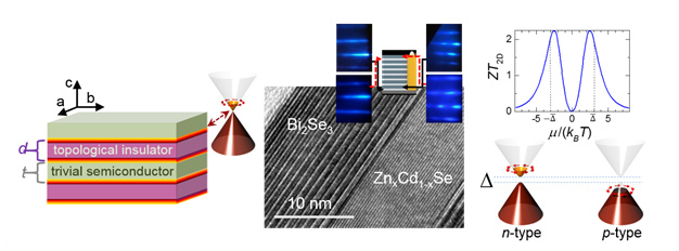
Cluster 1.1: Tunable topological hetero-nanostructures for thermoelectric applications. Thermoelectric materials interconvert thermal and electrical energy, and as such they may be used for both electrical refrigeration and power generation. Such materials will play an important role in our quest to find global sustainable energy solutions. This cluster aims to gain fundamental understanding and enhance thermoelectric performance of superlattice structures comprising periodic arrays of alternating topological insulator (TI) and trivial semiconducting (SC) materials [1-3]. It explores the unique properties [4] of the newly discovered TIs to boost thermoelectric figure of merit in TI/SC superlattice structures which our group was first to fabricate and to demonstrate robust topological properties at their interfaces.
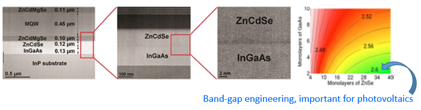
Cluster 1.2: Heterovalent II-VI/III-V semiconductor structures has a focus on sensing and photovoltaic applications. Heterovalent interfaces combine materials of different valence, such as ZnSe/GaAs, leading to structural and electronic properties that are unavailable with conventional materials containing isovalent interfaces [5,6]. They provide opportunities for new scientific discoveries and far-reaching technological impact. Members of the team have dramatically advanced the field of intersubband devices using heterovalent growth [7,8]. The goal of this cluster is to develop true heterovalent nanostructures and multilayers leading to new materials properties that will enable to realize applications in sensors and photovoltaics thus far not possible due to the current limits of isovalent nanostructures [9].
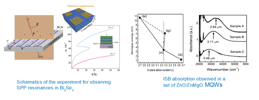
Cluster 1.3: Multi-layer nanostructures for novel photonic applications. This cluster explores two distinct paths to novel photonic device materials and structures. One involves MBE grown ZnO and related compounds [10,11]. ZnO is a material active in the deep UV spectral region and very promising for realization of exciton gain and development of efficient light emitters at room temperature and even at elevated temperatures. The aim is to establish electrically-pumped operation of near-IR intersubband optical emitters made from these oxide semiconductors. [12] The second path explores unique properties of topological surfaces of materials such as Bi2Se3 and Bi2Te3, to harvest their unique behaviors in plasmonic applications and allow coupling of light to the collective motion of Dirac plasmons in TI superlattices under various doping conditions [13,14].
References:
- Z. Chen, T. A. Garcia, J. D. Jesus, L. Zhao, H. Deng, J. Secor, M. Begliarbekov, L. Krusin-Elbaum, and M. C. Tamargo, Molecular beam epitaxial growth and properties of Bi2Se3 topological insulator layers using various substrate surface preparations, J. Electronic Mat. 43, 909 (2014).
- Z. Chen, T. A. Garcia, L. C. Hernandez-Mainet, L. Zhao, H. Deng, L. Krusin-Elbaum, and M. C. Tamargo, Molecular beam epitaxial growth and characterization of Bi2Se3/II-VI semiconductor heterostructures, Appl. Phys. Lett. 105, 242105 (2014).
- Z. Chen, L. Zhao, K. Park, T. A. Garcia, M. C. Tamargo, and L.Krusin-Elbaum, Robust topological interfaces and charge transfer in epitaxial Bi2Se3/II-VI semiconductor superlattices, Nano Lett., in review (2015).
- L. Zhao, H. Deng, I. Korzhovska, Z. Chen, M. Konczykowski, A. Hruban, V. Oganesyan and L. Krusin-Elbaum, Singular robust room-temperature spin response from topological Dirac fermions, Nature Materials, 13, 580 (2014).
- H. H. Farrell, M. C. Tamargo, J. L. de Miguel, F. S. Turco, D. M. Hwang, and R. E. Nahory ‘‘Designer’’ interfaces in II-VI/III-V polar heteroepitaxy, J. App. Phys. 69, 7021 (1991).
- J. Fan, X. Liu, J. K. Furdyna and Y. -H. Zhang, ZnTe/GaSb distributed Bragg reflectors grown on GaSb for mid-wave infrared optoelectronic applications, Appl. Phys. Lett. 101, 121909 (2012).
- Y. Yao, A. Alfaro-Martinez, K. J. Franz, W. O. Charles, A. Shen, M. C. Tamargo and C. F. Gmachl, Room temperature and narrow intersubband electroluminescence from ZnCdSe/ZnCdMgSe quantum cascade laser structures, App. Phys. Lett. 99, 041113 (2011).
- A. P. Ravikumar, T. A. Garcia, J. De Jesus, M. C. Tamargo, and C. F. Gmachl, High detectivity short-wavelength II-VI quantum cascade detector, App. Phys. Lett. 105, 061113 (2014)
- S. Agarwal, K. H. Montgomery, T. B. Boykin, G. Klimeck and J. M. Woodall, Design guidelines for true green LEDs and high efficiency photovoltaics using ZnSe/GaAs digital alloys,” Electrochem. Solid-State Lett. 13, H5-H7 (2010).
- K. Zhao, L. Ye, M.C. Tamargo, and A. Shen, Plasma-assisted MBE growth of ZnO on GaAs substrate with a ZnSe buffer layer, Phys. Status Solidi C9, 1809-1812 (2012).
- K. Zhao and A. Shen, Increasing ZnO growth rate by modifying oxygen plasma conditions in plasma-assisted molecular beam epitaxy, W. J. Cond. Matt. Phys. 2, 160 (2012).
- K. Zhao, G. Chen, B.-S. Li, and A. Shen, Mid-infrared intersubband absorptions in ZnO/ZnMgO multiple quantum wells, Appl. Phys. Lett. 104, 212104 (2014).
- J. A. Schuller, E. S. Barnard, W. Cai, Y. C. Jun, J. S. White, and M. L. Brongersma, Plasmonics for extreme light concentration and manipulation, Nat. Mater. 9, 193–204 (2010).
- P. Di Pietro, M. Ortolani, O. Limaj, A. Di Gaspare, V. Giliberti, F. Giorgianni, M. Brahlek, N. Bansal, N. Koirala, S. Oh, P. Calvani and S. Lupi, Observation of Dirac plasmons in a topological insulator, Nat. Nano. 8, 556 (2013).